December 2009 issue of German "Optik & Photonik" journal features Suss article on wafer-level camera manufacturing. According to the company, an estimated 80 million WLC modules have been delivered in 2009. The article goes in great lengths talking about background history behind the new micro-optics ideas, with natural emphasis on Suss contribution to the history.
The article also covers microlens imprint lithography (SMILE), where a liquid polymer is dispensed on the wafer and the lenses are imprinted by using a transparent stamp or mold and UV-light for curing. Master lens arrays consisting of aspherical microlenses with profile deviation below 50nm (rms) and surface roughness below 2nm (rms) were demonstrated on full 8" wafer scale by Suss MicroOptics. Recently Kaleido Technology, Denmark, presented a first 8" diamond milled lens master in brass, providing spherical, aspherical and free-form lenses with better than 2um lateral position accuracy.
The wafer-scale master wafers are then transferred into a soft stamp, usually made of Polydimethylsiloxane (PDMS) by casting. The PDMS layer serves as a stamp imprinting the shape on the microlens material. This material is not named by the article, other than saying that it's often kept in secret by the companies and now can be sourced from DELO, Germany and Asahi Kasei, Japan.
Another article from Fraunhofer Institute for Applied Optics and Precision Engineering talks about milling to produce wafer level optics, either directly or as a master for replication.
Thursday, December 31, 2009
iSuppli Q4 2009 Market Report
iSuppli published its Q4 2009 Image Sensors report. The market for area image sensors is predicted to decline from $7.4B and 1.4B units in 2008, to $6.0B and 1.3B units in 2009, resulting in a decrease of 15.5% in total area image sensor revenues in 2009.
DSCs remain the major application for CCDs, while mobile handsets use CMOS for mostly cost-sensitive reasons. Videoconferencing represents the second largest market application for CMOS sensors in terms of unit shipments, due to their inclusion in PC notebooks.
Mobile handsets are expected to remain the dominant application for CMOS sensors in the next five years as come 2013, 50 percent of total CMOS image sensor revenue will come from the mobile handset market, up from 43 percent in 2009. In terms of units, mobile handsets will account for approximately 78 percent of total CMOS image sensor units in 2009 and will occupy a similar amount five years from now.
ISuppli also presents a resolution trends chart:

Wednesday, December 30, 2009
Albert Theuwisen Reviews Year 2009
Albert Theuwissen published a review of 2009 and expectations from 2010 in Harvest Imaging blog:
"I heard from various industrial sources that CCD fabs as well as CMOS fabs are completely filled with image sensor wafers. Apparently the future for imaging looks bright.
Looking back to 2009, it was a difficult year for many of us in the imaging business."
"I heard from various industrial sources that CCD fabs as well as CMOS fabs are completely filled with image sensor wafers. Apparently the future for imaging looks bright.
Looking back to 2009, it was a difficult year for many of us in the imaging business."
ENG - Image Sensor Company from Japan
It came to my attention that is another small Japan-based company dealing with image sensor design - ENG. The name stands for "Exploitation of Next Generation". Although the company has started in 1992 and was active in different areas over the years, its only products these days are image sensors and related activities. The main differentiation of ENG sensors is high DR, up to 120db. All listed sensors are based on 7.65um pixels and have VGA resolution with 12b ADC.
With Brookman and Rosnes, ENG is the third small company in Japan dealing with CMOS sensor design.
With Brookman and Rosnes, ENG is the third small company in Japan dealing with CMOS sensor design.
Tuesday, December 29, 2009
Anteryon Mulls IPO in Q3 2010
KoersAlarl.nl, Het Financieele Dagblad and another article from Het Financieele Dagblad quote Dutch newspaper Financial Telegraaf saying that Anteryon considers IPO on the Amsterdam stock exchange (a part of Euronext exchange) or, less probably, on NASDAQ. Anteryon manufactures wafer-scale optics for Nokia, Samsung, LG, Sony Ericsson and Motorola camera phones.
Monday, December 28, 2009
Hynix Introduces VGA Sensor in ShellUT CSP Package
October Hynix newsletter presents a new VGA sensor in NeoPac CSP package from OptoPac. Hynix dubbed this package ShellUT. The sensor is based on 2.25um pixels, has 100mW typical power consumption and is supposed to go into mass production in Dec. 2009. It also has "anti-shake" feature to use in camera phones with G-sensor.
Thursday, December 24, 2009
Christmas Rumors
The rumors below are not confirmed and should be treated as such. Although I made some efforts to cross-check some of them, it does not guarantee their validity.
- Tower is preparing BSI image sensor process. If successful, Tower would become the second foundry, after TSMC, offering BSI process. So far BSI access was limited to big IDMs and selected TSMC customer club. Through Tower many more companies can start talking BSI.
- DxO Labs is in talks to sale the company (see August Rumors). Aptina is one of the potential buyers. Google is another one. Given the difference between Aptina and Google resources, I guess it's unlikely that Aptina's bid wins.
Now the interesting question is why Google needs DxO? My speculation is that DxO algorithms might be either integrated into Picasa or used to add nice camera features to Android platform.
- Meanwhile, Aptina and Finland-based Heptagon are considering a joint project on wafer-level camera development. Heptagon has close relationships with Nokia, so this project might give Aptina a leg up on winning the designs at Nokia.
- Sharp is considering to switch its new CMOS sensors development to TSMC. If this happens, TSMC CIS market share would not be solely based on Omnivision's one.
- SETi got big design win in Samsung handsets. With this win SETi starts its market expansion beyond China.
Toshiba Names CIS as One of the Top Priorities
Tech-On: Shozo Saito, Toshiba Semiconductor President, defines CMOS image sensors as one of the top priorities for its System IC Operation. Among the other priorities are analog, imagery and wireless chips. Saito also says that Toshiba currently hold the second-largest share worldwide in CMOS sensors - I guess it could be based on price, rather than unit volumes.
Wednesday, December 23, 2009
Caeleste, e2v, SensL Papers at CNES CMOS Detector Workship 2009
Caeleste published two new papers presented at the CNES CMOS Detector Workshop held on Dec 8-9 in Toulouse.
The first presentation covers e2v and Caeleste collaborative work on high-speed BSI sensor with large 24um 4T pixels. The sensor is manufactured by Tower in 0.18um process. The final product array size is 1680x1680 and it can be read out at 1000fps speed. The article talks about a smaller size prototype. 5.5um thick BSI substrate allows 90-95% peak QE.
The second presentation describes SensL, Caeleste and Vrije University of Brussels work on high speed SPAD photon counting array suitable for ToF sensing. The hybrid imager resolution is 128x2. The pixel size is 100x100um. With a nice analog time interpolation the sensor was able to achieve 154ps RMS time resolution or a little worse than 2cm range resolution. Each pixel has 479(!) transistors, including 15-bit time counter:
Micron Reports 13% Drop in CIS Foundry Revenues
Seeking Alpha published Micron's quarterly conference call for the quarter ended on Dec. 3, 2009 (first quarter in Micron's 2010 fiscal year).
Ron Foster, Micron CFO, said few words about the image sensor foundry business:
"Sales in memory products increased 38%, while sales of image sensors decreased 13%. Imaging revenue was $108 million in the first quarter and represented 6% of the Micron consolidated net sales. Recall of the first quarter results reflect our manufacturing services, including wafer fabrication to Aptina, following a spin off of that business in the fourth quarter. As I mentioned previously, we continue to account for our ownership interest in Aptina under the equity method of accounting."
TowerJazz Got General Dynamics and USAF ROIC Contract
Yahoo: TowerJazz announced its USA Aerospace and Defense Division has been awarded a contract by General Dynamics to support the MATES (MAnufacturing TEchnology Support) program within the U.S. Air Force for large-die read-out-integrated-circuit (ROIC) production.
The two year program with General Dynamics will focus on 0.18-micron large-die, stitched ROICs. In the 0.18-micron node, TowerJazz is making available to its ROIC customers a wide range of features from its commercial technology including high density capacitors (up to 5.6fF/um2), 1.8, 3.3, and 5V FETs, native devices, bipolar devices, resistors with near-zero temperature coefficients and a wide array of metal options. TowerJazz also provides cryogenic models for its devices to use in cooled ROIC designs.
The two year program with General Dynamics will focus on 0.18-micron large-die, stitched ROICs. In the 0.18-micron node, TowerJazz is making available to its ROIC customers a wide range of features from its commercial technology including high density capacitors (up to 5.6fF/um2), 1.8, 3.3, and 5V FETs, native devices, bipolar devices, resistors with near-zero temperature coefficients and a wide array of metal options. TowerJazz also provides cryogenic models for its devices to use in cooled ROIC designs.
Omnivision Won 5MP Slot in Next Generation iPhone
Digitimes: According to Digitimes sources, OmniVision has secured 5MP sensor orders for the next-generation iPhone, which will hit shelves sometime during the second half of 2010. Omnivision's iPhone sales are expected to grow to 40-45M units in 2010 from 20-21M (estimated) this year, according to the same sources. Including iPods, Omnivision's estimated total shipments to Apple are about 65M units in 2009.
OmniVision also supplies 3MP sensors for the current iPhone 3GS model. Aptina 2MP sensors were used in the previous generation iPhone 3G.
OmniVision also supplies 3MP sensors for the current iPhone 3GS model. Aptina 2MP sensors were used in the previous generation iPhone 3G.
Tuesday, December 22, 2009
Phase Profilometry for 3D Sensing
The open access Sensors Journal published an article on mathematics behind one of the techniques of the structured light 3D sensing (some call this approach active stereo, yet others call it triangulation):
A 3D Sensor Based on a Profilometrical Approach
Jesús Carlos Pedraza-Ortega, Efren Efren Gorrostieta-Hurtado, Manuel Delgado-Rosas, Sandra L. Canchola-Magdaleno, Juan Manuel Ramos-Arreguin, Marco A. Aceves Fernandez and Artemio Sotomayor-Olmedo
Facultad de Informatica, Universidad Autonoma de Queretaro, Av. de las Ciencias S/N, Juriquilla, C.P. 76230, Queretaro, Mexico
Abstract: An improved method which considers the use of Fourier and wavelet transform based analysis to infer and extract 3D information from an object by fringe projection on it is presented. This method requires a single image which contains a sinusoidal white light fringe pattern projected on it, and this pattern has a known spatial frequency and its information is used to avoid any discontinuities in the fringes with high frequency. Several computer simulations and experiments have been carried out to verify the analysis. The comparison between numerical simulations and experiments has proved the validity of this proposed method.
This article belongs to the special issue on Image Sensors. I'm not sure how this special issue is defined, as it has articles published a year ago, as well as quite recent ones - probably something to do with innovative open access publishing scheme. Another article belonging to this special issue is one mentioned a month ago on double exposure skimming HDR challenges.
Monday, December 21, 2009
Image Sensors for Kids
Wired: Those of us who'd like to see our kids continuing our imaging carriers, should look at Bigshot educational camera kit. The kit was created by Shree Nayar and a group of undergraduate and graduate students at the Computer Vision Lab at Columbia University.
Bigshot web site has quite a complete tutorial on all aspects of image sensor operation, showing Micron's 4T-shared pixel as an example (if you move the mouse over the picture).
Bigshot web site has quite a complete tutorial on all aspects of image sensor operation, showing Micron's 4T-shared pixel as an example (if you move the mouse over the picture).
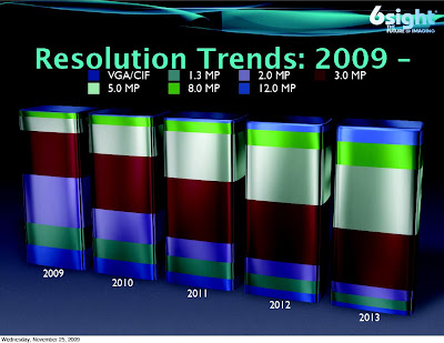
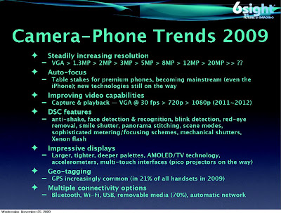
Tessera and Future Image at 6Sight Future of Imaging 2009
Below are some materials from 6Sight Future of Imaging Conference held on November 10-12, 2009 in Monterey, Calif.
Tony Henning, senior analyst from Future Image Inc., presented predictions on mobile imaging directions, including the camera-phone resolution trends:
Tessera presented its wafer level camera technology with sample pictures at 3MP resolution. The company claims that its technology is embedded in 2 out of 3 digital still cameras (I guess they mean Fotonation's image enhancing SW).
Update: The official conference web site is here. Videos of presentations and presentations in pdf form can be downloaded here.
Tony Henning, senior analyst from Future Image Inc., presented predictions on mobile imaging directions, including the camera-phone resolution trends:


Update: The official conference web site is here. Videos of presentations and presentations in pdf form can be downloaded here.
Sunday, December 20, 2009
FPN and Temporal Noise Effects on PTC
Albert Teuwissen continues his tutorial series on PTC as a tool for analyzing sensor imperfection. This part discusses FPN and temporal noises, such as 1/f, pixel thermal noise and kT/C residues.
Saturday, December 19, 2009
IEEE Spectrum Revisits CCD Nobel Controversion
December issue of IEEE Spectrum revisits the controversial story of CCD invention:
It's easy to see why the Nobel committee went with Boyle and Smith. The CCD is synonymous with its only practical application: imaging. And according to many authoritative sources, Boyle and Smith invented the CCD. But had the Nobel nominators looked one step down the chain of invention, things might have been different.
Carlo Séquin, now a professor of electrical engineering and computer science at the University of California, Berkeley, says: "If the fundamental concept was the charge-transfer principle, then that goes to Boyle and Smith, and maybe Gene Gordon." If it's the invention of a practical CCD imager, "credit would go to Mike Tompsett, and possibly Gilbert Amelio," he says. (Amelio led commercial CCD development at Fairchild Semiconductor.)
There are also references to Smith, Boyle and Gordon versions of the CCD invention story.
Friday, December 18, 2009
Pixart Optical Touch Panel Sales Up
Digitimes reports that Pixart's sales from its optical touch panel solutions for all-in-one PCs and notebooks will account for 5-10% of its total revenues in the fourth quarter of 2009, according to the paper sources.
Acer, HP, Lenovo and China-based Founder Technology have adopted Pixart's optical touch panels for their all-in-one PCs, and in 2010 they are expected to deliver a total of 6-7M optical touch panel modules from Quanta, Pixart's partner in optical touch development, the sources said. In addition, the Pixart solutions are being validated by Dell, which is likely to use them in its all-in-one PCs and notebooks next year, the sources added.
Acer, HP, Lenovo and China-based Founder Technology have adopted Pixart's optical touch panels for their all-in-one PCs, and in 2010 they are expected to deliver a total of 6-7M optical touch panel modules from Quanta, Pixart's partner in optical touch development, the sources said. In addition, the Pixart solutions are being validated by Dell, which is likely to use them in its all-in-one PCs and notebooks next year, the sources added.
Thursday, December 17, 2009
Omnivision Sensors in Blackberry Storm and Curve
EETAsia publishes reverse engineering article about Blackberry Storm revealing that it uses Omnivision's 3MP OV3647 packaged in 7mm x 7mm x 5mm module. The article also mentions that Blackberry Curve uses Omnivision sensor too - this time OV2640.
Omnivision Market Shares
Thanks to R.F. for pointing me to September Omnivision shareholders presentation with TSR-based market shares:


Update: There is also TSR projection of the total CMOS sensor market growth:


Update: There is also TSR projection of the total CMOS sensor market growth:

Wednesday, December 16, 2009
Aptina and eASIC Announce HD Video Reference Design
Yahoo: Aptina and eASIC announced the immediate availability of a H.264 HD reference design that is capable of supporting up to 720p/30fps rates. The design uses Aptina’s 2MP 1/3-inch MT9D131 SoC image sensor with eASIC’s eDV9200 low cost HD H.264 CODEC. The reference design enables video capture, H.264 compression and decompression, streaming of compressed AV streams through SPI or USB2.0, storage of compressed video and audio on a Secure Digital (SD) storage card, and decompression and playback on to LCD display or through a DVI interface.
The eDVR92-based H.264 HD reference design is available now from eASIC. Pricing for the eDVR9200 CODEC IC starts at $4.95 in high volume.
The eDVR92-based H.264 HD reference design is available now from eASIC. Pricing for the eDVR9200 CODEC IC starts at $4.95 in high volume.
Anteryon Wafer Level Optics Status
Anteryon published its wafer level optics status report at MEMSLand - a Dutch government-sponsored packaging program. Anteryon-based wafer level cameras can be found in Nokia 2330 phones. The slides below show Anteryon process flow and tolerances:


Broadcom Multimedia Processor Supports 1080p Video, 20MP Photo
Yahoo: Broadcom announced BCM2763 VideoCore IV multimedia processor supporting 1080p HD video and up to 20MP digital camera and photo image processing with advanced features such as multiple shots per second, image stabilization, face and smile detection and panorama mode. Broadcom uses 40nm process to achieve 490mW power for 1080p camcorder H.264 High Profile encoding and 160 mW for 1080p playback.
The BCM2763 is currently sampling to early access customers. Handsets utilizing the multimedia processor are expected to reach the market in 2011.
The BCM2763 is currently sampling to early access customers. Handsets utilizing the multimedia processor are expected to reach the market in 2011.
MIT Gesture Recognition Team Mulls Image Sensor in LCD Screen
Wired: The latest MIT gesture recognition system uses an array of optical sensors that are arranged right behind a grid of liquid crystals. The sensors can capture the image of a finger when it is pressed against the screen. But as the finger moves away the image gets blurred.
By displacing the layer of optical sensors slightly relative to the liquid crystals array, the researchers can modulate the light reaching the sensors and use it capture depth information, among other things.
In this case, the liquid crystals serve as a lens and help generate a black-and-white pattern that lets light through to the sensors. That pattern alternates rapidly with whatever the image that the LCD is displaying, so the viewer doesn’t notice the pattern.
The pattern also allows the system to decode the images better, capturing the same depth information that a pinhole array would, but doing it much more quickly, say the MIT researchers.
MIT researchers haven’t been able to get LCDs with built-in optical sensors to test, though they say companies such as Sharp and Planar have plans to produce them soon.
For now, doctoral candidate Matthew Hirsch and his colleagues at MIT have mocked up a display in the lab to run their experiments. The mockup uses a camera that is placed some distance from the screen to record the images that pass through the blocks of black-and-white squares. MIT will present the idea at the Siggraph conference on Dec. 19.
Tuesday, December 15, 2009
Nemotek Added Test Capabilities
EETimes: Morocco-based Tessera licensee Nemotek announced in-house WLC test capabilities. The tests are performed in Class 10 clean room and include the module leakage currents, depth, resolution, distortion, signal-to-noise ratio and color accuracy.
Sony 0.9um Pixel Presentation at IEDM 2009
Image sensor blog from Japan puts together few words about Sony presentation at IEDM 2009 titled "0.9um Pitch Pixel CMOS Image Sensor Design Methodology".
As far as I was able to understand, Sony built 0.9um, 1.12um, 1.4um and 1.75um pixels using 0.18um FEOL and 65um copper BEOL process. All the pixels are FSI, rather than BSI. The pixels design was based on simulation results optimizing microlens shape, stack hight and metal opening.
1.1um pixel performance was considered OK. 0.9um pixel QE was unacceptably low. The article also mentions SNR10 being of order of 100Lux, not clear for what pixel size.
Monday, December 14, 2009
Surveillance Sensor Market to Go Down
In-Stat predicts that image sensor revenue across all surveillance cameras will decline from over $700M in 2008 to $435M in 2013.
Overall semiconductor revenue for the video surveillance equipment will be relatively flat between 2009 and 2013, as lower average selling prices (ASPs) offset unit shipment growth. The video encoder/image processors will be the dominant semiconductor segment as it shifts from MPEG-4 part 2 to H.264.
Overall semiconductor revenue for the video surveillance equipment will be relatively flat between 2009 and 2013, as lower average selling prices (ASPs) offset unit shipment growth. The video encoder/image processors will be the dominant semiconductor segment as it shifts from MPEG-4 part 2 to H.264.
Friday, December 11, 2009
Optrima Forms 3D Technology Alliances
This is a news from about a month ago, I missed it at the time. There appears to be a 3D imaging alliance between Belgim-based Optrima, Melexis, Softkinetic and the US Texas Instruments.
Optrima is a Vrije University of Brussels spin-off pursuing 3D TOF hardware, including 3D TOF sensors, cameras and platforms. Optrima was founded in April 2009. It appears there is an alliance between Melexis and Optrima on automotive 3D sensors. The two companies presented 3D TOF embedded camera for automotive applications at 2009 International Automotive Electronic Congress on November 17-18 in Paris.
On the gesture recognition front Optrima formed a joint venture with Softkinetic, a provider of software for gesture recognition. Softkinetic-Optrima venture offers two ToF cameras together with SDK.
The newly formed JV announced a collaboration with TI to design, develop and market joint 3D imaging solutions for the television, personal computers, digital signage, health & fitness, industrial, robotics, automotive, security and many others markets.
Recently Softkinetic also announced support for Panasonic 3D cameras - an indication that Panasonic is getting serious about ToF sensors. “The new 3D Image Sensor is the result of years of development and improvements at Panasonic that led to our background light suppression technology. Panasonic’s sensor has very competitive specifications, and is perfectly fit for all the out-of-home digital applications,” said Mr. Yuji Takada, General Manager, Research & Development Center at Panasonic Electric Works.
Thursday, December 10, 2009
Omnivision High Full Well Photodiode
Omnivision patent application US20090302358 discloses a technique to increase the photodiode full well capacity in 4T pixel. The proposal is to reduce a transfer gate sidewall spacer closest to the photodiode, as shown on the figure below:

One may ask how this increases the full well of photodiode? Here is the explanation:
In the conventional process for fabricating a CIS, after the gate layer has been formed, the PD region is implanted next to the gate of the transfer transistor. After the PD region is implanted, but before the sidewall spacers of the transfer transistors are formed, the pinning layer is implanted. This order of fabrication provides pinning under the sidewall spacers, which helps to reduce dark current and white pixels. However, the thermal processing for sidewall spacer formation also causes the P type dopants of the pinning layer to diffuse, resulting in a less abrupt p-n junction and therefore a lower full-well-capacity.
In the Omnivision's proposal the abrupt junction of pinning layer is achieved by reordering the implanting pinning layer step to be after formation of sidewall spacers. To compensate for process reordering, thinned sidewall spacer is thinned relative to regular sidewall spacer. Sometimes the thinned sidewall spacer could be entirely removed.

Wednesday, December 09, 2009
Pixart to Apply Its Optical Touchscreen to Smartphones
Digitimes reports that Pixart plans to step into the market of optical finger navigation (OFN) solutions for smartphones. OFN is expected to be widely adopted by international handset vendors to control smartphone screens in 2010. Pixart will face strong competition from Avago and ST, according to Digitimes sources.
Tuesday, December 08, 2009
Rosnes Comes with Products
It came to my attention that Kyoto, Japan-based image sensor start-up Rosnes come up with many products. The camera module products are in a pdf catalog in English, while image sensor chip list is in Japanese. Rosnes sensors appear to be based on 1.75um and 3um pixels with resolution range spanning from VGA to 5MP, some with integrated ISP - quite a lot of products for a less than 3 year old company! The company also offers custom design and IP services.
The company information page says that Rosnes was established in January 2007. Takumi Yamaguchi, Rosnes' President, reportedly came from Panasonic. The company investors are Daiwa SMBC Capital, Nissei Capital, and NTT Finance.
The company information page says that Rosnes was established in January 2007. Takumi Yamaguchi, Rosnes' President, reportedly came from Panasonic. The company investors are Daiwa SMBC Capital, Nissei Capital, and NTT Finance.
Sunday, December 06, 2009
Image Sensors in Brazil
Albert Theuwissen gives a nice overview of image sensor activity in Brazil in his blog:
At this moment the overall semiconductor activities in Brazil are continuously growing, but there is still very limited work going on in the field of imagers. A few start-up companies are doing quite nice work, but they do not (yet) reach the level of the companies present in North America, Europe or the Far East.
At this moment the overall semiconductor activities in Brazil are continuously growing, but there is still very limited work going on in the field of imagers. A few start-up companies are doing quite nice work, but they do not (yet) reach the level of the companies present in North America, Europe or the Far East.
Thursday, December 03, 2009
Organic SWIR Sensors
Electron and Holes blogger spotted an interesting Laser Focus article on SWIR image sensor made of organic materials. The pixels are based on hybrid diodes with colloidal lead sulfide (PbS) quantum dots. A ternary composite of electron- and hole-conducting organic semiconductor blended with the colloidal QDs to yield highly sensitive SWIR photodiodes.

The devices achieved external quantum efficiencies (EQEs) of up to 51%. With glass-encapsulated hybrid diodes and operating at room temperature, the 256x256 pixel imager is sensitive up to 1.9 µm. Its pixel pitch is 154um. The whole work was done by Siemens, Germany.
Wednesday, December 02, 2009
Aptina to Expand China Market Presence
Digitimes: Aptina is gearing up to tap China's white-box handset market with new VGA sensors, according to Digitimes' sources. The company has introduced the VGA CIS A390, which has relatively lower efficiency compared to its A380 or A360 but a more competitive price (the products under these names can not be found on the company's web site). Aptina recently made sample shipments to customers in China, Digitimes' sources indicated.
Aptina used to only take orders for high-end handset products provided by first-tier vendors, but now it decided to go to the lower tiers. On the Chinese market it will compete primarily with Omnivision and SETi.
Aptina used to only take orders for high-end handset products provided by first-tier vendors, but now it decided to go to the lower tiers. On the Chinese market it will compete primarily with Omnivision and SETi.
Tuesday, December 01, 2009
Quanta to Equip 70% of its PCs by Pixart's Touchscreen in 2010
Digitimes: Quanta optical touchscreen-based all-in-one PCs are estimated to account for more than 70% of the company's four million total shipments in 2010, according to Digitimes sources. According to the earlier Digitimes' report, Pixart is Quanta Computer's sole supplier of sensors for optical touch screens.
Currently, Quanta ships about 150,000-200,000 touchscreen-based all-in-one PCs every month.
Currently, Quanta ships about 150,000-200,000 touchscreen-based all-in-one PCs every month.
Omnivision Quarterly Earnings Call
Seeking Alpha published transcript of Omnivision's quarterly earnings call for the quarter ended on Oct. 31, 2009. The company's revenues reached $183 million representing sequential growth of 74% over the previous quarter. Gross margin also improved to 24% for the last quarter from 22.4% in the previous one. Omnivision's cash and short term investments at quarter end increased to $354 million.
Some interesting quotes form the call:
Shaw Hong, CEO:
...we are actively designing our second generation Omni BSI 2 pixel technologies while our competitors are still trying to deliver their first generation technology.
Ray Cisneros, VP Sales:
In the [recent] quarter we shipped approximately 145 million units at an average selling price of $1.27. This compares with approximately 75 million units shipped in the [previous] quarter at an average selling price of $1.40. Sequential revenue growth was driven by our strong position in the Smart Phone handset market, mainstream handset market and notebook market. The sequential decline in ASP is the result of an exceptionally strong demand in the mainstream handset market that drove a revenue mix shift towards lower resolution products.
...we secured significant inroads into the Japanese market for digital video camera application using our 8 megapixel BSI product... Our 5 megapixel BSI products have also secured multiple design wins in the digital still camera market and shipments began in the third quarter.
Q&A session:
Quinn Bolton – Needham & Company:
...Shaw in your closing remarks said that the CameraCube and Omni BSI were now shipping to multiple Tier One’s. Can you give us a sense of when you think those revenues will become material contributors to revenue?
Ray Cisneros:
We are extremely excited about the traction we have in design wins with customers buying our CameraCube. It is tangible. It is material, albeit a very small percentage right now. The way it is working out to be, most of these cameras are backing into the secondary camera application and handsets so therefore the actual mass or volume of this particular camera is not as large as the primary camera. Going forward we expect to transition this technology into primary camera applications but that has yet to be plans laid out or openly discussed yet so we are still very excited about this whole trend.
Yair Reiner – Oppenheimer:
Shifting over to China, you mentioned some strategy for dealing with more competition in China before. Can you talk a little bit about what some of those strategies might be?
Ray Cisneros:
As Bruce mentioned in his script there is the launch of our new VGA 7675. It is I would say the best, bar none, balance between cost and performance. The other strategy we have been talking about here is the CameraCube for secondary camera applications. Going forward there are other strategies we need to take into action as we go forward because the China market as we mentioned we feel has expanded because of its infrastructure and readiness to basically change business models globally.
Subscribe to:
Posts (Atom)